Research Areas
Scanning probe techniques
Scanning probe microscopy (SPM) is a family of mechanical probe microscopes including scanning tunneling microscopy and atomic force microscopy (AFM) that measures surface morphology in real space with a resolution down to the atomic level. Contact mode AFM is a mechanical probe technique capable of mapping real-space 3-demensional surface morphology and properties such as friction force, adhesion force and elasticity.
In the dynamic force AFM mode, the tip-sample interaction is controlled by maintaining a reduced amplitude of a vibrating cantilever driven by a piezo element while the tip scans the sample surface. Under this feedback mechanism, the phase lag between the vibrating cantilever detected by the photodetector and the driver signal, referred to as phase shift, is sensitive to both mechanical and chemical properties of the sample. Mapping of the phase shift (simultaneously with the topographic image), known as phase imaging technique, has found applications in studies of soft materials.
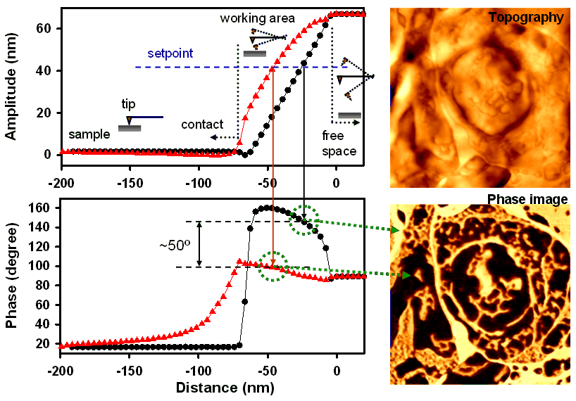
Our research activities include visualization of biological structures present on unfixed rat brain sections and additives in polymer composites with phase shift imaging. Shown above is the topographic image and phase image (scan area is 5 micron square) obtained on the surface of an unfixed rat brain section, as well as amplitude- and phase-distance curves. The contrast in phase image is a reflection fact that the energy dissipation of the vibrating cantilever/tip ensemble is dependent on the mechanical properties of the probed area.
The interactions between the probe and the sample surface contain information in regard to viscoelasticity, surface chemistry and other properties. Because this is a two-body interaction, both the sample and probe contribute to the outcome of their interaction. We are interested in controlling the surface chemistry of AFM tips. Silicon probes are inherently hydrophilic, making them prone to "sticky" contaminants such as organic and inorganic oxides. A tip modified with hydrophobic coatings such as self-assembled monolayrs will likely solve this type of problems.
SPM is used to measure surface features at nanometerscales because silicon probes have a sharp tip (apex radius ~10 nm). However, when the size of surface features are comparable to the tip apex itself, the geometry of the tip apex will be convoluted to the image. When the tip apex is larger than the surface features, the image is no longer a reflection of the sample; rather, it is dominated by the tip geometry. Understanding this nature of AFM is important in properly interpreting images, especially for nanometer-scale features.
Time-of-flight secondary ion mass spectrometry
By measuring mass to charge ratios (m/z) of secondary ion fragments generated from the bombardment of a sample surface by a primary ion beam (e.g., Bi3+), ToF-SIMS is a powerful tool in identifying molecules by detecting molecular ion fragments and/or a number of characteristic fragments. Its applications include verification and/or identification of surface contaminants. For example, a common surface contaminant is silicone oil or polydimethylsiloxane, which has been found to result in a group of ion fragments serving as fingerprints (for example, positive secondary ions at m/z 28, 73, 147, 207, 221 and 281, which are assigned to Si+, SiC3H9+, Si2C5H15O+, Si3C5H15O3+, Si3C7H21O2+ and Si4C7H21O4+, respectively).
With another ion gun used to sputter the surface, ToF-SIMS is capable of depth profiling, for example, thin oxide layers of metals and layered structures of electronic and optical films. It also has imaging capacity because a full spectrum is collected over each pixel of the rastered area: an image of a selected ion fragment is generated by plotting its intensity against the pixels.
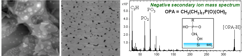
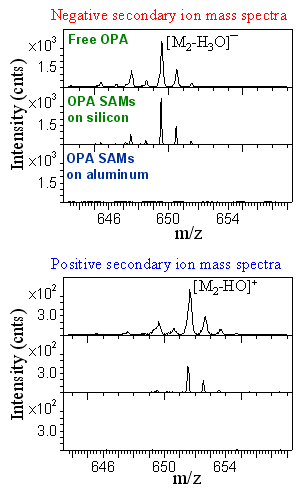
This surface analytical technique can also be used to explore how molecules are attached to a substrate by pondering (data mining) the fragmentation of the molecules themselves and their association with the substrate. For example, as shown in the right, for octadecylphosphonic acid (OPA, or ODPA) SAMs spin-coated on silicon and aluminum oxides, ToF-SIMS revealed that ion fragmentation of the OPA molecules (C18H39PO3, represented by M) is distinctive: on silicon oxide, there are condensed dimers of [M2-H2O]- and [M2-HO]+; by contrast, there are no such ion fragments detected on aluminum oxide. OPA powders (can be called free OPA and the molecules are bonded by H-bonding between the headgroups and van der Waals forces between the alkyl chains) rendered same ion fragmentation as OPA SAMs on silicon, suggesting that the molecules in the SAMs are bonded by H-bonding with the substrate. The lack of these condensed dimers, plus other difference in ion fragmentation found between OPA SAMs on silicon and on aluminum oxides, prove that the OPA SAMs are covalently bonded to aluminum oxide.
Self-assembled monolayers (SAMs)
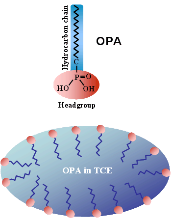
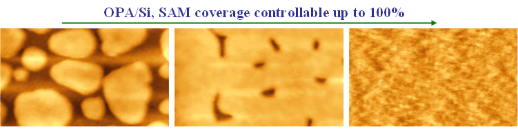
Via use of appropriate non-polar solvents having a dielectric constant of ~4, we developed a novel method of delivering& OPA SAMs on a surface that is hydrophilic. In this method, as shown in the schematic to the right, the solvent (trichloroethylene, TCE) is used as an active medium to force the molecular headgroups to concentrate on the medium surface, leading to a fast growth of SAMs, as well as formation of SAMs that either have a covalent bond or H-bonding with an oxide, depending on the nature of the interaction between the OPA molecular headgroup and the substrate. Shown below is an example of formation of full-coverage OPA SAMs on silicon oxide by adding solution during spin-coating.
Because of this solvent-assisted mechanism, the only requirement for SAM formation is physical contact between the OPA-loaded medium and a
hydrophilic substrate. This leads to an extremely fast growth rate allowing spin-coating SAMs on a hydrophilic substrate. The utility
of this method has been demonstrated by other researchers in modifying the gate dielectric surface before depositing the active organic
semiconductor in organic thin-film transistors (OTFTs) for improving device performance.
Our objective in this research area is surface engineering at the molecular level with SAMs and utilizing such a well-controlled surface to construct patterned surface chemistry for manipulation of chemical and biological interactions.
Updated on October 12, 2021.