STM | AFM | Contact AFM | Force curve | Lateral force | Force modulation | Local modification
Non-contact AFM | Phase imaging | Magnetic force | Surface potential | Check AFM tips
Cleaning by UVO | Conclusion | Other info
spacing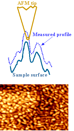
Scanning probe microscopy (SPM) is a family of mechanical probe microscopes that measure surface morphology in real space with spatial resolution down to the atomic level. SPM originated from scanning tunneling microscopy (STM), in which the electrical current arising from electron tunneling between a sharp tip and a sample surface is used as the feedback signal to maintain a well-defined separation between them. Invented in 1981, STM introduced a fundamentally new capability: direct imaging of atomic arrangements on surfaces in real space. Its profound impact on science and technology related to surface phenomena was recognized when the inventors of STM shared the Nobel Prize in Physics in Physics in 1986 with the inventor of electron microscopy.
Because STM requires both the tip and the sample to be electrically conductive, it cannot be applied to poorly conducting or insulating materials. To overcome this limitation, atomic force microscopy (AFM) was developed in 1986 to enable high-resolution surface characterization of nonconductive materials. Since then, AFM has evolved rapidly and found far broader applications than STM across many scientific and engineering fields. Today, nearly all types of materials can be studied using AFM. In addition to surface morphology, SPM techniques have been extended to probe a wide range of surface properties, including chemical, electrical, magnetic, and mechanical characteristics. This diversity arises from the fact that the probe tip is either in contact with, or in close proximity to, the sample surface, allowing various tip–sample interactions to be accessed and measured.
Return to Top
1. STM
The basic principle of scanning tunneling microscopy (STM) is conceptually simple: electron tunneling between two electrodes under an applied electric field. Translating this quantum-mechanical phenomenon into a practical technique capable of imaging surfaces with atomic resolution, however, posed significant technical challenges.
To measure the tunneling current, the separation between the tip and the sample must be controlled to within approximately 1 nm. Achieving such precision requires atomically clean surfaces and an extremely stable, vibration-free measurement system. Shown here is an STM image acquired on a highly oriented pyrolytic graphite (HOPG) substrate.
Quantum mechanics predicts that the tunneling current depends exponentially on the distance between the two electrodes. Experimental verification of this relationship, demonstrated in 1981 between a tungsten (W) tip and a platinum (Pt) surface by G. Binnig, H. Rohrer, Ch. Gerber, and E. Weibel, is regarded as the birth of STM. The subsequent achievement of atomic-resolution imaging on a Si(111) 7×7 reconstructed surface in 1982 is often considered a major breakthrough in STM instrumentation. Since then, an extensive body of literature has emerged, reflecting the rapid development and widespread adoption of STM.
As a research tool, STM has been used primarily to investigate atomic-scale surface structure and electronic properties of solid surfaces, typically under ultrahigh vacuum (UHV) conditions. Beyond imaging, STM also enables the manipulation of individual atoms, as demonstrated in an IBM video illustrating atom-by-atom positioning on a surface.
How STM works?
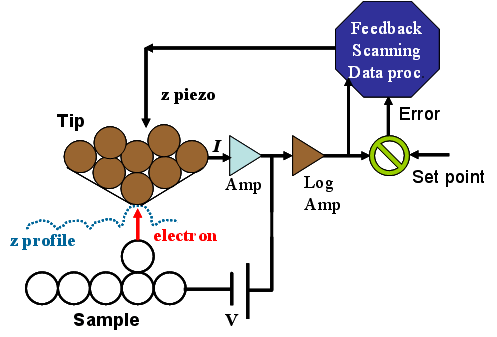
Shown here is a schematic diagram illustrating the operating principle of STM. By approaching the tip toward the sample under a specified bias voltage and target tunneling current, the tip is positioned at a distance from the surface such that the prescribed current (the setpoint) is maintained. As the tip is scanned laterally across the surface under this condition, the system continuously compares the measured tunneling current I with the setpoint current Is. The difference between them (I − Is) serves as the error signal in a feedback loop, which applies an appropriate voltage to the z‑piezo actuator to adjust the tip–sample separation and minimize the error (I − Is ≈ 0). The resulting z‑piezo displacement as a function of lateral position provides a height profile representing the surface “topography.” This mode of operation is known as constant-current mode.
In the alternative constant-height mode, the tip–sample distance is held fixed while variations in the tunneling current are recorded during scanning. Because no feedback correction is applied in the z direction, this mode requires the scanned area to be atomically flat to avoid tip–sample contact and potential damage.
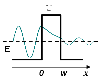
To elucidate the tunneling of electrons between the tip and the sample, we introduce a model describing electrons confined within a potential well and analyze their ability to tunnel through an adjacent potential barrier.
Shown here is the wavefunction of electrons confined in a potential well and its exponential decay into the barrier, which gives rise to tunneling to the opposite side. The wave nature of electrons is described by the Schrödinger equation, shown below:
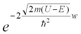
By enforcing the continuity of the electron wavefunctions and their first derivatives across the three regions—the potential well, the barrier (whose width is w), and the region beyond the barrier—the probability of electron transmission through the barrier is
which is proportional to the tunneling current. It therefore follows that the tunneling current increases exponentially as the tip–sample separation decreases. which is proportional to the tunneling current. It therefore follows that the tunneling current increases exponentially as the tip–sample separation decreases.For a typical metal with an average work function of approximately 4 eV, the tunneling current I can be expressed as e-2w with w in Å.
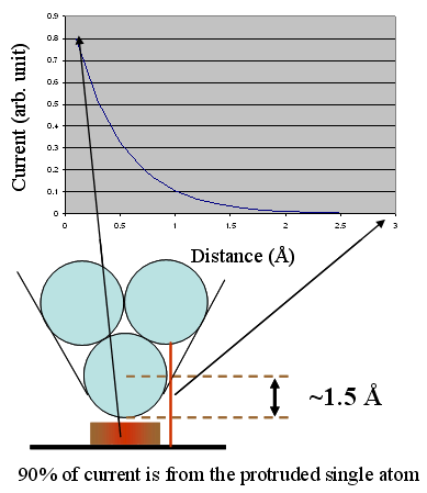
A rough estimation illustrates how sensitively the tunneling current depends on the tip–sample distance. When the separation changes by 1 Å, the tunneling current typically varies by a factor of 7.3–10. This extreme distance sensitivity underlies the physics that enables STM.
Consider an STM tip terminated by a single atom with an effective radius of approximately 1.5 Å. The next atom behind it is therefore about 2.6 Å farther away from the sample surface. Its contribution to the tunneling current is reduced by a factor of e-5.2, corresponding to only about 0.6% of the current contributed by the apex atom. As a result, the tunneling current is dominated by the foremost atom at the tip apex. This pronounced sensitivity of the tunneling current to distance makes STM an imaging technique capable of true atomic resolution—provided that high-quality tips and well-prepared sample surfaces are used.
2. AFM
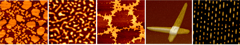
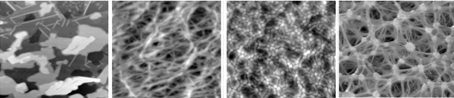
Examples of AFM images obtained on four different samples To achieve spatial resolution comparable to that of STM on insulating surfaces, atomic force microscopy (AFM) was invented in 1985 by G. Binnig, C. F. Quate, and Ch. Gerber, as reported in their seminal 1986 paper. In the first implementation of AFM, an STM was used to detect the deflection of a flexible cantilever, allowing measurement of the contact force between the AFM tip and the sample surface. In modern AFM systems, however, cantilever deflection is most commonly detected using an optical beam‑deflection scheme.
A sharp tip with an apex radius of approximately 10 nm, formed on a flexible cantilever, is used to probe the interaction forces between the tip and the sample surface. The tip–sample interaction can be described using the Lennard–Jones potential, which characterizes the interaction between two atoms:
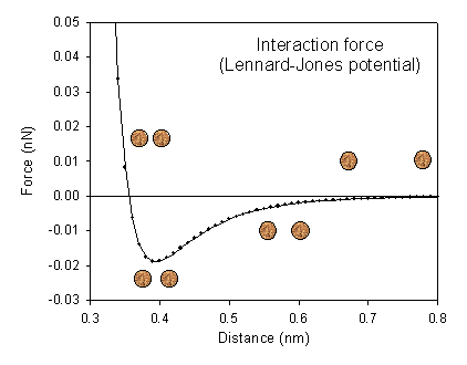
w(r) = −A/r6 + B/r12,
where r is the separation between the two atoms, and A and B are interaction constants. The corresponding interaction force is obtained by differentiating the potential with respect to distance:
F(r) = −dw(r)/dr = −6A/r7 + 12B/r13.
According to standard textbook values, the constants A and B are on the order of 10−77 J m6 and 10−134 J m12, respectively. A calculated force–distance curve based on these parameters is shown to the right. At a separation distance of approximately 0.4 nm, a weak attractive force dominates. As the separation decreases further, the repulsive force rises steeply, reflecting the strong short‑range repulsion between atoms.
In practice, the attractive force between an AFM tip and a sample surface can be much larger than that predicted by the simple two‑atom model described above. This is primarily because the AFM tip, with a typical radius of ~10 nm, is significantly larger than an individual atom, resulting in the collective interaction of many atoms at the tip apex with the surface. In addition, longer‑range forces—such as capillary forces arising from adsorbed water layers and electrostatic forces due to surface charges or potential differences—often contribute substantially to the overall tip–sample interaction.
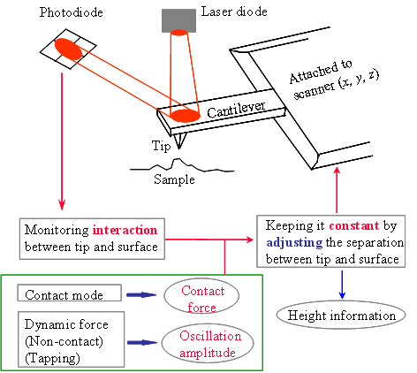
The operating principle of AFM is illustrated below. AFM functions by maintaining a constant interaction between the tip and the sample surface through a feedback system that continuously adjusts the tip–sample separation. Depending on which tip–sample interaction is used as the feedback signal, two primary imaging modes are commonly employed: contact mode and dynamic force mode.
The interaction force between the tip and the sample surface is detected by measuring the deflection of the cantilever. This is typically achieved using an optical beam‑deflection scheme, in which a laser diode illuminates the back of the cantilever and the reflected beam is detected by a position‑sensitive photodiode. A quadrant photodiode enables simultaneous measurement of both cantilever deflection and torsion. These signals are used to determine the normal force acting on the tip as well as the lateral (friction) force experienced by the tip as it scans across the sample surface.
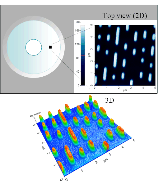
While scanning the tip across the sample surface (x, y), the system adjusts the distance (z, which is thus the measure of the height of the sample surface features) between the tip and the sample surface to maintain a constant contact force (contact mode) or oscillation amplitude (dynamic force mode). A 3-D image is thus constructed by the lateral dimension the tip scans and the height the system measures. Shown below is an example of AFM image obtained on a stamp. The 3D rendering of the AFM image is in a false color scale.
By combining the lateral scan coordinates with the measured vertical displacement, a three‑dimensional representation of the surface topography is constructed. Shown below is an example of an AFM image acquired on a CD master stamp (a precision nickel mold used in CD replication to emboss nanoscale data patterns into polycarbonate disc). The three‑dimensional rendering of this AFM image is displayed using a false‑color scale to enhance visualization of surface features.
2.1 Contact Mode AFM
In contact‑mode AFM, the tip is in mechanical contact with the sample surface.
This is illustrated in the figure to the left, where the tip is shown both in free space and in contact with the surface. When the tip is pressed against the sample, the cantilever bends upward. If the cantilever deflection is denoted by z, the force exerted on the sample surface is given by F = kcz, where kc is the spring constant of the cantilever.
The deflection of the cantilever is measured using an optical detection scheme. A laser beam is focused onto the free end of the cantilever (near the tip), and the reflected beam is detected by a position‑sensitive photodetector. Changes in the position of the reflected laser beam correspond directly to the cantilever deflection, allowing precise measurement of the tip–sample interaction force.
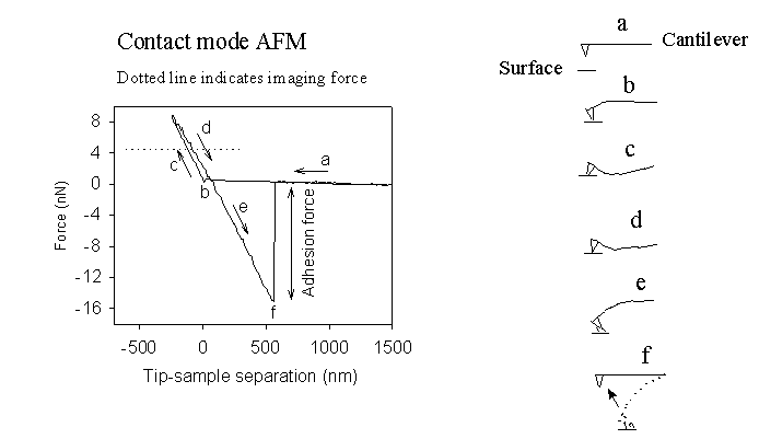
The applied force kcz can be evaluated from a force–distance curve, which is obtained by bringing the tip toward the sample surface and subsequently retracting it, as shown below. The insets in the figure illustrate the tip–sample interactions corresponding to different regions of the force–distance curve, as detected through cantilever deflection.
When the tip is far from the surface, there is no measurable interaction between the tip and the sample (a). As the tip approaches the surface, an attractive force develops between them. In contact‑mode AFM, the gradient of this attractive force is typically much larger than the spring constant of the cantilever (usually < 1 N/m). As a result, the tip becomes unstable and snaps into contact with the surface (b).
Further extension of the tip results in a repulsive (loading) force as the cantilever bends upward while the tip remains in contact with the surface (c). The repulsive force region is commonly used as the feedback signal in contact‑mode AFM to map surface morphology. Forces on the order of a few nanonewtons are typically applied during contact‑mode imaging.
During the retraction cycle (d and e), adhesion forces established between the tip and the surface prevent immediate separation. The tip remains attached to the surface until the restoring force of the cantilever exceeds the adhesion force (f), at which point the tip detaches. This minimum force required to separate the tip from the surface, known as the pull‑off force, provides a quantitative measure of the adhesion between the AFM tip and the sample surface.
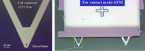
A very soft cantilever with a spring constant of approximately 0.1 N/m is typically used in contact‑mode AFM. An optical photograph of such a cantilever is shown below. Because the cantilever is extremely compliant, it can be pulled into contact with the sample surface when attractive tip–sample forces are present. In practice, the gradient of the attractive force between the tip and the surface (on the order of ~10 N/m) is usually much larger than the spring constant of these soft cantilevers, leading to a spontaneous jump‑to‑contact behavior.
After mechanical contact is established between the tip and the sample surface, a repulsive interaction force develops between them. In contact‑mode AFM, this repulsive force is used as the feedback parameter. By maintaining a constant force through continuous adjustment of the sample (or tip) height while the tip scans across the surface, the AFM system records the vertical displacement required to preserve this condition, thereby generating an image of the surface morphology.
Because the AFM tip is in mechanical contact with the sample surface in contact‑mode operation, a variety of surface properties can be measured simultaneously with the topographic image. These include friction force distributions and mechanical properties such as stiffness and wear behavior. In addition, by precisely controlling the applied normal force, contact‑mode AFM can be used for nanolithography on certain materials. A solid understanding of force–distance curves is therefore essential for correctly interpreting contact‑mode AFM images and for diagnosing imaging artifacts or failures, particularly when experimental conditions deviate from ideal operation.
2.1.1 Force-Distance Curves
Force–distance curves are obtained by extending the AFM tip toward the sample surface until mechanical contact is established, followed by retracting the tip away from the surface. The reference point for the tip–sample distance is commonly defined as the point of mechanical contact during the approach (extension) cycle. Further extension of the tip beyond this point results in a loading force applied to the surface.
The slope of the loading region of the force–distance curve reflects the mechanical response of the sample and can be used to estimate its Young’s modulus. This measured response, however, is often convoluted with the spring constant of the cantilever. Consequently, to accurately determine the Young’s modulus of a sample, it is important to select a cantilever whose spring constant is comparable to the effective stiffness of the surface being measured.
During the retraction cycle of a force–distance measurement, adhesion between the AFM tip and the sample surface prevents immediate separation. As a result, the tip remains attached to the surface until the restoring force applied during retraction exceeds the adhesion force between the tip and the sample. The force required to detach the tip from the surface, known as the pull‑off force, provides a quantitative measure of the adhesion between the tip and the surface.
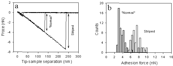
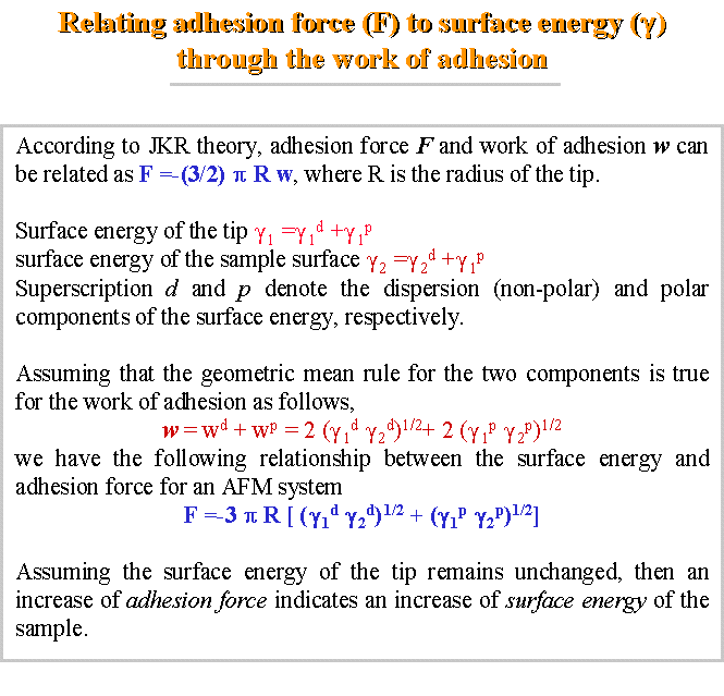
The adhesion force is related to the surface energies of both the tip and the sample, as well as their interfacial energy. Shown below is an example of adhesion force measurements obtained at different regions on a biaxially oriented polypropylene (BOPP) film. The striped regions, which were mechanically scratched, exhibit higher adhesion forces than the undamaged surface. As will be discussed later, this enhanced adhesion is also correlated with increased friction force contrast observed in friction force microscopy images.
Click here to see an example of increased adhesion force measured on UV/ozone‑treated polypropylene films. Adhesion force can be related to the surface energies of both the AFM tip and the sample surface, as well as their interfacial energy. In cases where liquid‑like contaminants or adsorbed moisture layers are present on the sample surface, capillary forces must also be taken into account.
Force–distance measurements have been extended beyond conventional surface characterization to probe molecular-scale interactions. These techniques have demonstrated the ability to record events such as (a) the rupture of a single molecular bond, referred to as single-molecule force spectroscopy, and (b) the folding and unfolding of proteins by mechanically confining individual molecules between the AFM tip and the sample surface.
2.1.2 Lateral Force Microscopy (LFM)
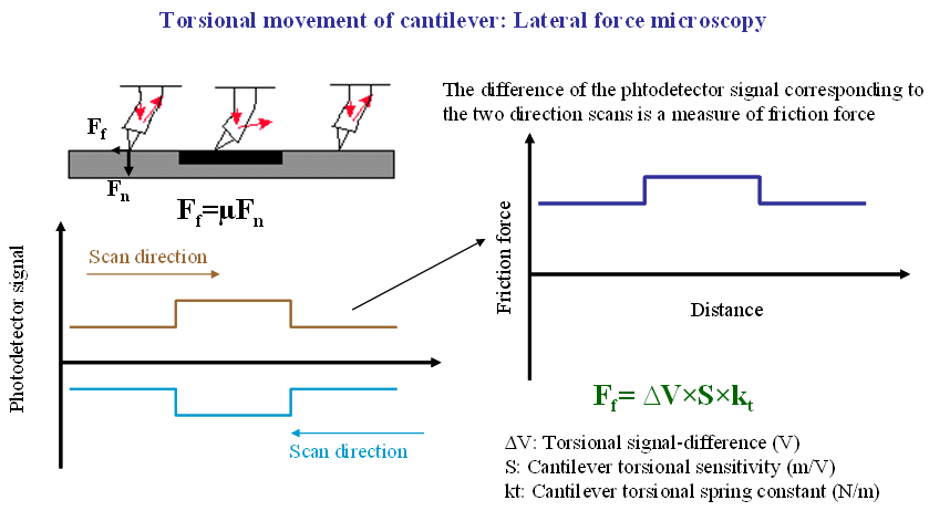
Lateral force microscopy (LFM) is based on measuring the torsional motion of the AFM cantilever as the tip scans across the sample surface, as illustrated below. This torsional deflection arises from lateral forces acting on the tip and is commonly used to map variations in friction across a surface. As indicated in the figure, the difference between lateral force signals acquired during forward and backward scans yields a friction force image.
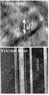
Friction force imaging can be used to distinguish regions with different surface properties, such as hydrophilicity, based on differences in their interactions with the AFM tip. Shown here is an example in which higher friction forces are observed on scratched regions of a BOPP film. This enhanced friction is attributed to the higher surface energy of the mechanically damaged areas. Corresponding force–distance curves acquired on the normal and striped (scratched) regions are shown above and demonstrate that the observed friction force contrast is closely related to differences in adhesion between the tip and the surface.
Friction force measurements can also be used to detect chemical functional groups on a surface when the AFM tip is modified with specific chemical functionalities, a technique known as chemical force microscopy (CFM). Common functional groups used for tip modification include hydroxyl (OH) and carboxyl (COOH) groups. For example, a commercially available silicon tip is naturally terminated with a native silicon oxide (SiO2) layer, rendering the tip hydrophilic.
Such a hydrophilic tip can be used to distinguish the chemical amphiphilicity of octadecylphosphonic acid (OPA) molecular layers. Specifically, a surface terminated by hydrophilic headgroups exhibits a larger friction force than a surface terminated by hydrophobic alkyl tails. When friction force imaging is combined with topographic height measurements, it becomes possible to determine whether an amphiphilic molecular film consists of an even‑numbered multilayer (terminated by headgroups) or an odd‑numbered multilayer (terminated by tail groups).
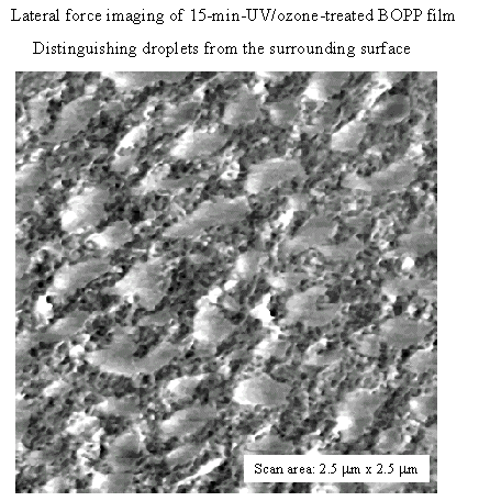
On the other hand, lateral force imaging can also reveal local topographic variations through enhanced torsional motion of the cantilever when the tip scans across edges or boundaries of surface features. Such contrast arises because abrupt height changes increase lateral forces acting on the tip. Click here to see an LFM image obtained on a polypropylene film treated with UV/ozone for 15 minutes, in which surface droplets are clearly distinguished from the surrounding regions.
This capability makes lateral force microscopy particularly useful for identifying different phases on surfaces exhibiting relatively large height variations, a situation frequently encountered in practical surface analysis.
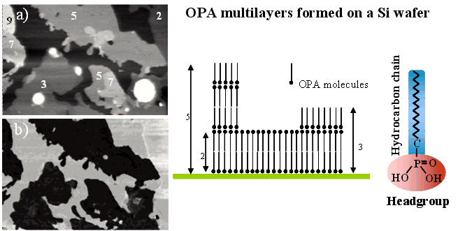
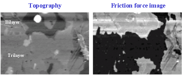
Shown below is an example of a friction force microscopy study of multilayers of OPA, formed on a silicon wafer. The topographic image in (a) (scan area: 14.0 μm × 8.8 μm) reveals the formation of a bilayer as well as odd‑numbered multilayers. The numbers in (a) denote the number of molecular layers present in each multilayer region.
The corresponding friction force image in (b) shows that the bilayer and the exposed silicon substrate exhibit similar friction forces, both of which are higher than those measured on the multilayer regions. This friction contrast reflects differences in surface termination: the bilayer is terminated by the polar OPA headgroups, which interact more strongly with the hydrophilic silicon tip coated with a native SiO₂ layer, whereas the odd‑numbered multilayers are terminated by nonpolar methyl (CH₃) groups. As a result, regions with headgroup termination display higher friction than those terminated by hydrophobic alkyl chains.
2.1.3 Force Modulation
In addition to mapping surface topography, AFM can be used to probe local elastic properties of materials through mechanical interactions between the tip and the sample surface. As illustrated below, this can be achieved by applying a small oscillation to the sample height while measuring the corresponding response of the cantilever using a lock‑in amplification technique. This approach effectively measures the slope of the force–distance curve in the repulsive force regime, which is directly related to the local elastic modulus of the material. As a result, variations in surface elasticity can be distinguished and spatially mapped using this technique.
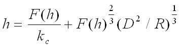
Let h be the displacement of the piezo actuator, p the deflection of the cantilever, and d the penetration depth of the tip into the sample. These quantities are related by h = p + d. If the spring constant of the cantilever is kc, the force F exerted on the tip can be calculated from the cantilever deflection as F = kcp. According to the Hertzian contact model, the penetration depth d is related to the applied force F, the probe radius R, and the elastic properties of the tip and sample by d = F2/3(D2/R)1/3, where D is the reduced Young’s modulus, determined by the Young’s moduli of the tip (Et) and the sample (Es), as well as the Poisson’s ratio σ: D = 3(1 − σ2)(1/Es + 1/Et)/4. For polymer samples, the Young’s modulus of the sample is typically much smaller than that of the tip (Es << Et). Under this condition, D can be approximated as D = 3(1 − σ2)/(4Es).
Using the relations above, the dependence of the piezo displacement h on the applied force F can be written as follows:
In practice, the experimental method measures dF/dh, the slope of the force–displacement curve, which serves as a measure of the Young’s modulus of the sample.
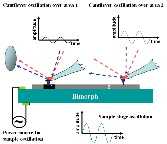
The oscillation of the sample height can be implemented by applying a sinusoidal voltage from a function generator to the z‑direction of the piezoelectric (PZT) scanner on which the sample is mounted.
This sinusoidal excitation drives the piezo scanner to oscillate the sample height with a peak‑to‑peak amplitude of approximately 1 nm. The response of the cantilever to this modulation is detected using a lock‑in amplifier and is used to generate images related to the local elasticity of the sample surface.
As long as the oscillation frequency of the sample height is higher than the cutoff frequency of the feedback loop, this modulation does not affect the topographic imaging. Consequently, surface topography and elasticity distribution images can be acquired simultaneously.
An example of elasticity mapping of a polystyrene (PS) and polystyrene/poly(ethylene oxide) (PS/PEO) blend film spin‑coated on a mica substrate, obtained using a cantilever with a spring constant of 0.75 N/m, is shown in the figure to the left.
The mechanism of force‑modulation imaging is illustrated using force–distance curves (a) acquired on mica and polystyrene (PS) surfaces, together with the simultaneously recorded cantilever response (b) to a sample‑height oscillation with an amplitude of 1 nm at a frequency of 5 kHz. The cantilever used in this experiment had a spring constant of 18 N/m, and the tip approach and retraction speed was 3 nm/s.
The difference observed in the cantilever response shown in (b) arises from the different slopes of the force–distance curves in (a) measured on the two materials. These slope differences directly reflect the large contrast in Young’s moduli between mica (~200 GPa) and polystyrene (~5 GPa).
2.1.4 Locally Modifying Surfaces
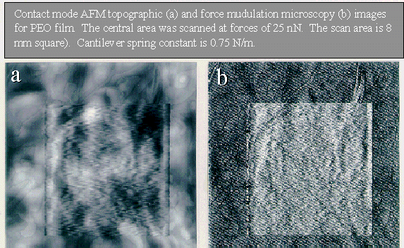
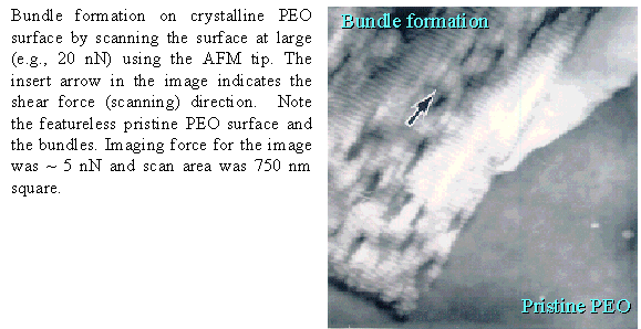
Surface structures can be intentionally modified by applying sufficiently large forces through the AFM tip while scanning across the surface. This capability has been exploited as a form of nanolithography for creating nanometer‑scale structures with spatial control. For example, on crystallized PEO thin films, both the surface morphology and local elastic properties were modified by the action of the AFM tip. A detailed view of the AFM‑induced modification of the PEO surface is shown here.
2.2 Dynamic Force Mode AFM Techniques
Dynamic force AFM (also known as tapping‑mode or non‑contact AFM) employs a cantilever that oscillates near its resonant frequency to probe surface features. This technique was originally developed to minimize surface damage and tip wear commonly encountered in contact‑mode AFM, particularly when imaging soft or weakly bound materials.
To understand the interaction between an oscillating AFM tip and the sample surface, it is useful to first examine the equation of motion of a driven cantilever in free space, where no tip–sample interaction is present. In this case, the cantilever is subjected only to an external driving force of the form F0cos(ωt). The dynamics of the cantilever—namely, its vertical displacement z as a function of time t—can be modeled as a point mass attached to a spring and damper, as described by the following equation of motion:
With the definitions ω02 = k/m and c = mω0/Q, where ω0 is the angular resonant frequency of the cantilever and Q is the quality factor, the equation of motion can be rewritten as:
This second‑order, nonlinear differential equation admits a steady‑state solution in which the cantilever oscillates sinusoidally at the driving frequency:
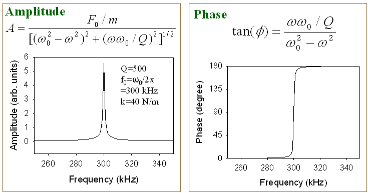
where A is the amplitude of the oscillation and φ is the phase lag relative to the driving force. Both quantities are illustrated below using a numerical simulation.
From the simulation shown above, it is evident that significant cantilever oscillation occurs only when the driving frequency is close to the resonant frequency of the cantilever. The simulation also shows a sharp change in the phase lag at resonance. In dynamic force AFM, tip–sample interaction forces effectively modify the resonance frequency of the cantilever, which in turn alters the oscillation amplitude.
In practice, as illustrated in the figure below, the oscillation amplitude decreases as the tip–sample separation is reduced. Because the tip–sample interaction force is complex and strongly nonlinear, there is generally no analytical solution to the equation of motion when this force is included. Nevertheless, numerical simulations have been shown to reproduce the experimentally observed dependence of oscillation amplitude on tip–sample distance (see, for example, A. San Paulo and R. Garcia, 471, Surface Science 471, 71 (2001)).
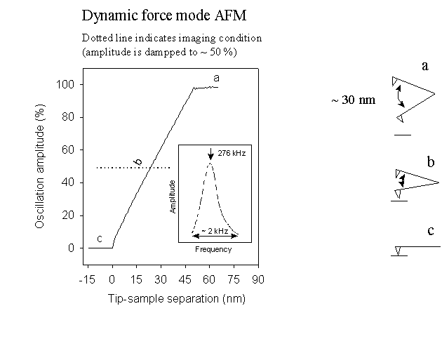
In dynamic force mode AFM, silicon cantilevers with spring constants typically ranging from 5 to 40 N/m are used. A representative cantilever with a spring constant of 40 N/m has dimensions of approximately 125 µm in length, 30 µm in width, and 3.7 µm in thickness. In this mode of operation, a reduced oscillation amplitude is used as the feedback parameter. The change in oscillation amplitude as a function of tip–sample distance, measured on a BOPP film, is shown below. The dominant tip–sample interactions occurring at different tip–sample distances are indicated by the insets labeled (a)–(c)
The figure above shows that when the AFM tip is far from the sample surface (a), the cantilever oscillates with a constant amplitude, corresponding to the free‑space condition where no tip–sample interaction exists. As the tip approaches the surface and enters the range of attractive and/or repulsive interactions, the oscillation amplitude begins to decrease (b). When the tip is brought into mechanical contact with the surface, the cantilever oscillation is completely suppressed (c).
Dynamic force mode AFM operates by scanning the oscillating tip across the sample surface while continuously adjusting the tip–sample separation to maintain a constant reduced oscillation amplitude, typically a fixed fraction (e.g., 50%) of the free‑space amplitude. This feedback‑controlled adjustment of the tip–sample distance enables the construction of a surface topographic image. Based on this general operating principle, a variety of dynamic AFM modes have been developed to probe different surface properties, as discussed in the following sections.
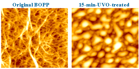
The AFM images shown here clearly illustrate the formation of mound-like surface features on UV/ozone-treated biaxially oriented polypropylene (BOPP) films, whereas the untreated surface is characterized by a fiber-like network morphology. The images were acquired over a scan area of 2 µm × 2 µm with a height range of approximately 25 nm. In addition to the morphological changes, an increase in adhesion force is observed on the treated surface. This enhanced adhesion indicates an increase in surface energy, which can be attributed to oxidation of the polymer surface induced by the UV/ozone treatment.
When the oscillation amplitude is relatively large (for example, greater than ~2 nm), the AFM tip intermittently makes contact with the sample surface during each oscillation cycle. This intermittent contact is the reason this technique is commonly referred to as dynamic force mode or tapping‑mode AFM. In practical imaging of relatively large areas, a larger oscillation amplitude is often employed because it provides improved stability and robustness against tip–sample adhesion and surface contamination.
Most dynamic force mode AFM systems described above operate in the amplitude‑modulation (AM) mode, in which changes in oscillation amplitude serve as the feedback signal. When the oscillation amplitude is very small (on the order of a few nanometers or less), the tip may no longer physically tap the surface, and the technique is then referred to as non‑contact AFM. In this regime, the tip senses long‑range attractive interactions without making mechanical contact with the surface. Non‑contact AFM is typically operated under ultrahigh vacuum (UHV) conditions and employs frequency‑modulation (FM) techniques to achieve true atomic‑resolution imaging.
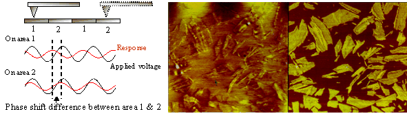
2.2.1 Phase Shift Imaging
The phase shift of an oscillating AFM cantilever is highly sensitive to tip–surface interactions, which are often material‑specific and influenced by factors such as surface chemistry and viscoelasticity. As a result, phase‑shift contrast in tapping‑mode AFM can be used to distinguish different surface compositions and material domains, as illustrated in the schematic below. A variety of surface properties may contribute to phase contrast, including differences in friction, adhesion, viscoelastic response, and material composition.
Phase imaging often provides strong and intuitive contrast when measurable differences in surface properties are present. However, interpretation of phase‑shift images must be approached with care, as the observed contrast may reflect a combination of multiple interacting factors. Reliable interpretation therefore typically relies on complementary measurements and prior knowledge of the sample system. Despite this complexity, phase imaging is a particularly powerful and valuable technique in SPM research, as it frequently reveals previously unrecognized surface heterogeneity and enables discovery of new physical or chemical phenomena.
Applications of phase imaging include visualization of phase separation in polymer blends, identification of filler distribution in polymer nanocomposites, and mapping of surface chemical variations. Shown below are a topographic image (left) and a corresponding phase‑shift image (right) of a toner particle consisting of a carbon black matrix with polymer fillers (scan area: 3.5 µm × 3.5 µm).
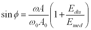
Phase shift is sensitive to tip–sample interaction, which is why phase-shift imaging is a powerful technique for differentiating component materials on a surface. According to Cleveland et al. and Garcia et al., the phase-shift angle φ is related to energy dissipation during tip–sample interactions (Edis), which reflects differences in material properties, as well as to hydrodynamic damping in the surrounding medium (Emed).
In amplitude-modulated AFM, a cantilever oscillating at angular frequency ω (with ω0 being the angular resonance frequency) has a free oscillation amplitude A0 and a reduced setpoint amplitude A. Under these conditions, the phase lag φ is given by:
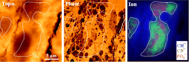
Shown below is an example demonstrating the use of phase-shift imaging to visualize intracellular organelles in a sectioned rat brain. The brain tissue was not chemically fixed prior to imaging, thereby preserving its native surface chemistry. The AFM topographic and phase-shift images shown below were acquired from neurons in the CA1 region of the rat hippocampus using a brain section with a thickness of 30 µm.
Also shown are overlaid time-of-flight secondary ion mass spectrometry (ToF-SIMS) negative secondary ion images of CH¯, CN¯, and PO2¯. These ion images were obtained using a Bi3+ primary ion beam operated in high spatial resolution (burst-alignment) mode. The white guide lines inserted in the images highlight organelles that are resolved by both AFM phase-shift imaging and ToF-SIMS, demonstrating strong correlation between nanoscale mechanical/chemical contrast and chemical composition.
The topographic image provides little information about intracellular organelles. In contrast, the phase‑shift image clearly reveals organelles as darker regions, indicating that these subcellular features are mechanically softer than the surrounding areas. Because organelles are rich in phospholipids, which exhibit liquid‑like and viscoelastic behavior, they are expected to dissipate more energy from the oscillating AFM probe. Conversely, the brighter regions in the phase image are likely composed of dried proteins and salts, which are relatively stiff materials and therefore dissipate less energy during probe oscillation.
These interpretations of the phase-shift contrast are supported by the ToF-SIMS ion images. In particular, the PO2¯ signal is representative of phospholipids and nucleic acids, while the CN¯ signal is characteristic of protein-rich regions. The spatial correlation between the phase-shift contrast and the chemical ion images provides strong evidence that phase imaging sensitively reflects differences in subcellular composition and mechanical properties.
2.2.2 Magnetic Force Microscopy (MFM)
Magnetic domains can be visualized using AFM when a magnetized tip is employed, a technique known as magnetic force microscopy (MFM). In MFM operation, topographic information is first acquired for each scan line using dynamic force mode AFM. The tip is then lifted to a fixed height above the surface (typically on the order of ~50 nm) and the same scan line is retraced.
At this lifted height, long‑range magnetic forces between the magnetized tip and the sample surface cause changes in the oscillation amplitude or phase of the cantilever. These changes are used to map the spatial distribution of magnetic forces, thereby revealing magnetic domain structures. MFM is widely used to investigate magnetic force distributions in recorded magnetic media (data storage devices) as well as micromagnetic structures in magnetic materials. For additional details and applications of this technique, readers are referred to the cited literature.
2.2.3 Electric Force Microscopy (EFM)
Similar to magnetic force microscopy (MFM), electrostatic force microscopy (EFM) employs a conductive AFM tip to probe variations in the electric field gradient above a sample surface. In EFM, long‑range electrostatic interactions between the biased conductive tip and the surface lead to changes in the oscillation amplitude, phase, or resonance frequency of the cantilever. Mapping these changes enables visualization of spatial variations in surface charge, dielectric properties, or electric potential. EFM has proven particularly useful in failure analysis of integrated circuits (ICs), where it can identify charge accumulation, dielectric breakdown, and other electrically active defects.
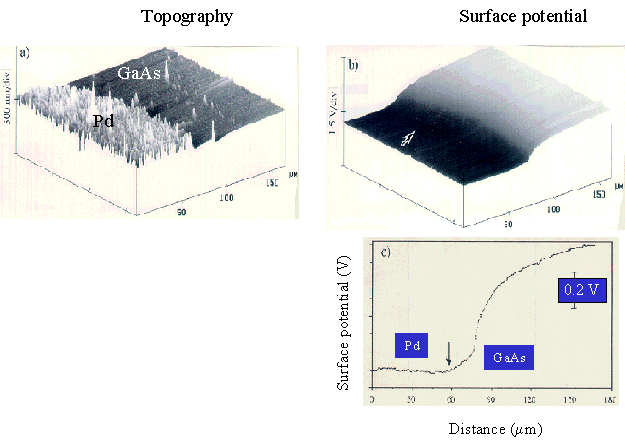
2.2.4 Scanning Surface Potential Microscopy (SSPM)
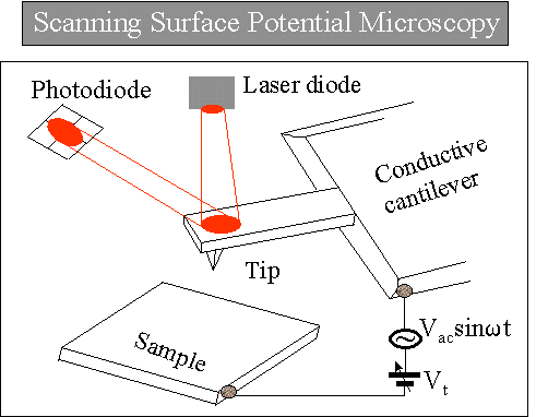
This technique maps the local surface potential distribution simultaneously with surface topography by maintaining a fixed separation between the sample surface and a conductive AFM tip biased with a sinusoidal voltage. The operating principle of scanning surface potential microscopy (SSPM) is illustrated in the figure on the right. When a potential difference exists between the tip and the sample surface, an oscillating electrostatic force is generated at the same frequency as the applied sinusoidal voltage.
This force induces an oscillatory motion of the cantilever, which is used as the feedback signal. The control system minimizes this oscillation by applying an appropriate DC voltage to the tip, thereby nullifying the potential difference between the tip and the surface beneath it. The required DC voltage is equal to the local surface potential at the tip position. By recording this voltage during scanning, a surface potential map is obtained simultaneously with the topographic image.
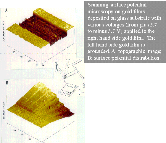
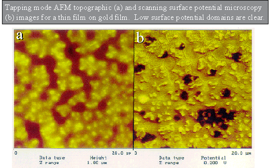
As shown in the figure to the left, gold films deposited on a glass substrate were used to validate the operation of SSPM. A potential difference between the two gold films was established by independently biasing them. During scanning, the applied bias was varied so that different potential differences between the two gold regions were measured and recorded, demonstrating the ability of SSPM to accurately map surface potential variations.
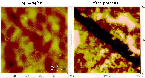
Deposition of a metal such as palladium (Pd) onto a semiconductor provides another example of surface potential contrast, arising from the formation of a metal–semiconductor contact potential. Shown here is a measurement of the contact potential difference between Pd and a semiconductor surface. Additional examples of surface potential mapping include measurements on a Pd (110) single‑crystal surface and on thin films, both exhibiting clear spatial variations in surface potential.
3. A Simple Method to Check AFM Tip Performance Using a Polymer Film
3.1 BOPP film surface for tip radius evaluation
An AFM image is formed by detecting interactions between the apex of the probe tip and surface features during scanning. This interaction—whether it is a contact force, oscillation amplitude, phase shift, or another measurable signal—serves as the feedback parameter used to regulate the separation between the tip and the sample surface. Because of this imaging mechanism, an AFM image is, in practice, a convolution of the tip geometry and the true surface topography. As illustrated below, the effective probe in AFM imaging is determined by the relative sharpness of the tip apex and the surface features: whichever is sharper dominates the measured image.
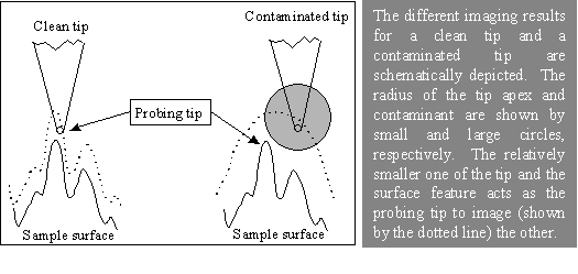
In practice, the AFM tip apex may be contaminated or damaged, for example by the attachment of a relatively large particle. In such cases, surface features that are sharper than the effective tip apex may themselves act as the probing element. As a result, images acquired with a contaminated or blunted tip can be dominated by the geometry of the tip rather than the true surface morphology, a phenomenon often referred to as tip self‑imaging. If this tip effect is not carefully considered, interpretation of AFM images can be highly misleading.
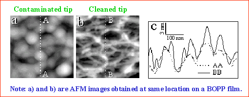
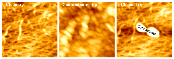
To ensure reliable imaging, it is therefore essential to verify that the AFM tip is sufficiently sharp and clean. This can be accomplished using reference samples with well‑defined and known surface features that are suitable for evaluating tip performance. Introduced here is a simple and effective method based on imaging a BOPP film, which exhibits nanometer‑scale fibrous surface structures. The BOPP film serves as a useful reference because a contaminated or damaged tip fails to resolve the fine fiber‑like network, as illustrated in the figure below. Successful imaging of this delicate fibrous structure provides a practical criterion for assessing tip quality. Many other reference samples with known geometries can likewise be used to characterize AFM tip shape and performance.
Because the polymer film is much softer than the silicon AFM tip (the Young’s modulus of polypropylene is ~1–2 GPa, whereas that of silicon is ~132–190 GPa), the polymer surface does not damage the tip when the tip is pressed into it. As illustrated in the figure below, this mechanical contrast can be exploited to clean a contaminated AFM tip. By gently pushing the tip into the polymer surface, contaminants adhered to the tip apex can be removed without blunting or damaging the tip.
An additional advantage of BOPP films is their highly hydrophobic nature and very low surface energy, approximately 30 mJ/m². For comparison, the surface energy of silicon oxide is ~70 mJ/m², and the surface tension of water is 72 mN/m. The low surface energy of BOPP helps prevent contaminants from accumulating on the polymer surface, thereby minimizing recontamination of the tip during evaluation and cleaning. This dual use of BOPP films for both AFM tip performance evaluation and tip cleaning was highlighted in the April 1, 2001 issue of Analytical Chemistry.
3.2 Applications of blind tip reconstruction
Considerable effort has been devoted to mathematically extracting the geometry of an AFM tip directly from an image using algorithmic approaches collectively known as blind tip reconstruction. This methodology is based on the key assumption that protrusions observed in an AFM image represent self‑imaging of the tip. In other words, surface features that are sharper than the tip apex effectively act as probes, thereby revealing information about the tip geometry itself.
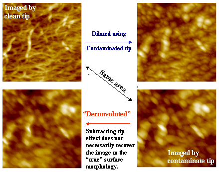
Blind tip reconstruction has proven to be both useful and effective for estimating tip shape from existing AFM images, provided that appropriate samples are used—specifically, samples containing surface features sharper than the tip. Once the tip geometry is determined, its influence on the acquired image can be removed through a mathematical operation known as erosion, or equivalently, deconvolution. Conversely, dilation is a related operation that adds the tip effect to an existing AFM image by virtually “scanning” a known tip shape across the image surface. This approach is particularly useful for simulating tip artifacts, as the AFM imaging process itself can be fundamentally regarded as a dilation operation between the tip geometry and the true surface features of the sample.
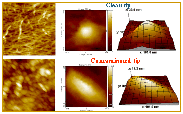
We have demonstrated that BOPP films are well suited both for evaluating AFM tip performance and for cleaning contaminated tips. This capability enables the acquisition of AFM images from the same area of a BOPP surface before and after the tip has been cleaned. Under these conditions, any differences between the two images can be attributed solely to contamination of the tip.
We took advantage of this capability by imaging the same surface area with the same AFM tip in two states: first while the tip was contaminated, and subsequently after it had been cleaned using the BOPP film. The commercial software package SPIP (Metrology Image ApS, Denmark) was used to estimate the tip geometry via its Tip Characterization Module, which implements a blind tip reconstruction algorithm. Blind reconstruction was first applied to the image acquired with the contaminated tip, allowing the geometry of the tip to be extracted directly from the image data. Once the contaminated tip geometry was estimated, it was used to simulate the tip‑convolution effect on the image acquired with the cleaned tip. By comparing the simulated image with the image obtained using the contaminated tip, we demonstrated that the blind tip reconstruction procedure accurately captures the tip geometry and effectively reproduces the observed imaging artifacts.
A comparison between tip geometries obtained from blind tip reconstruction and from scanning electron microscopy (SEM) images was previously reported by Dongmo et al. [J. Vac. Sci. Technol. B 14, 1552 (1996)]. In contrast, we developed a simpler and more direct approach to evaluate the validity of blind reconstruction by comparing AFM images collected from the same area of a BOPP film using a clean tip and a contaminated tip.
If the estimated geometry of the contaminated tip obtained through blind reconstruction is accurate, one should be able to use this geometry to dilate the AFM image collected with the clean tip, thereby generating an image that closely resembles the one acquired with the contaminated tip. Conversely, the effectiveness of deconvolution can be assessed by eroding the image collected with the contaminated tip using the reconstructed tip geometry and determining whether the result resembles the image obtained with the clean tip. Agreement in both cases provides strong validation of the blind reconstruction approach and its ability to accurately capture the tip‑convolution effect in AFM imaging.
Because an AFM image is a convolution of the true surface features and the geometry of the probe tip, when neither component is known a priori, it is impossible to determine whether an image of an unknown sample is dominated by surface morphology or by tip artifacts. When the tip apex is significantly sharper than the surface features, the resulting image more closely represents the “true” surface topography. This is why the use of a reference sample is essential for evaluating AFM tip performance.
It is also important to recognize that AFM tips can be easily contaminated or damaged, depending on the chemical and mechanical properties of the sample surface being examined. Although electron microscopy can be used to assess the outline of a tip from selected viewing directions, it is difficult—if not impossible—to directly measure the full three‑dimensional geometry of the tip apex. In this context, the combination of blind tip reconstruction with the use of a BOPP reference film provides a simple and effective protocol for testing the accuracy of tip‑geometry estimation for a contaminated tip. This can be achieved by comparing the image acquired using the contaminated tip with an image generated by dilating the image collected using a clean tip with the reconstructed tip geometry.
On the other hand, when the AFM tip is significantly larger than the surface features, scanning with such a tip produces an image that primarily reflects the geometry of the tip apex itself rather than the true surface morphology. In this situation, information about the actual surface features is physically lost during image acquisition. Consequently, applying an erosion (deconvolution) operation cannot fully recover the “true” surface structure, although the mathematical transformation may yield an image that more closely approximates it. The extent to which surface features can be recovered through erosion depends on the severity of tip contamination and the degree to which the image is dominated by tip effects. In extreme cases, fundamentally different surface morphologies may produce nearly identical AFM images when scanned with a highly blunted or contaminated tip, as the observed contrast is governed almost entirely by the tip geometry.
H.-Y. Nie, M.J. Walzak and N.S. McIntyre, Atomic force microscopy study of biaxially-oriented polypropylene films, J. Mater. Eng. Perform., 13, pp.451-460 (2004). H.-Y. Nie, M.J. Walzak and N.S. McIntyre, Use of biaxially-oriented polypropylene film for evaluating and cleaning contaminated atomic force microscopy probe tips: An application to blind tip reconstruction, Rev. Sci. Instrum. 73, pp.3831-3836 (2002). H.-Y. Nie and N.S. McIntyre, A simple and effective method of evaluating atomic force microscopy tip performance, Langmuir 17, pp.432-436 (2001).
4. A General Method for Cleaning Contaminated AFM Tips Using UV/Ozone Treatment
AFM probe tips can become contaminated either during scanning of certain sample surfaces or simply through prolonged exposure to ambient air. Such contamination is typically recognized by unstable imaging conditions and degraded image quality. When a tip exhibited these symptoms, it was removed from the AFM system and subjected to a 5‑minute UV/ozone treatment. After this treatment, imaging stability was restored and image quality improved significantly. These observations demonstrate that UV/ozone treatment is an effective method for cleaning contaminated AFM tips and provides a practical approach for extending and recycling probe tip usage.
The ultraviolet radiation emitted by a mercury lamp used in UV/ozone systems consists primarily of light at 253.7 nm, with a much smaller contribution at 184.9 nm. Photons at both wavelengths are effective in the removal of organic contaminants from surfaces.
Ozone can be generated by irradiating molecular oxygen (air) with short‑wavelength UV light at 184.9 nm, which has a photon energy of 6.70 eV (154.59 kcal/mol). However, to achieve sufficiently high ozone concentrations for rapid cleaning, a separate ozone source—such as an ozone generator—is typically required. The primary active species responsible for rapid contaminant removal is atomic oxygen, which is produced by photodissociation of ozone under irradiation with 253.7 nm UV light (photon energy 4.89 eV or 112.66 kcal/mol). Atomic oxygen is a highly reactive oxidizing agent that converts organic contaminants into volatile species, which are subsequently desorbed from the surface.
In addition, UV irradiation directly excites organic contaminant molecules, increasing their chemical reactivity toward ozone and atomic oxygen. While ozone alone can oxidize organic contaminants, the combined UV/ozone process is substantially faster and more efficient than ozone treatment alone.
5. Concluding Remarks
Scanning probe microscopy (SPM) techniques constitute a powerful and versatile platform for nanoscience and nanotechnology. Their ability to probe, manipulate, and modify materials at the nanometer and even atomic scale has led to widespread adoption across many scientific and engineering disciplines. An increasing number of researchers are using SPM not only as an imaging tool, but also as a means of fabricating and characterizing nanoscale structures and devices.
SPM continues to play a key role in advancing fundamental understanding in physics, chemistry, materials science, and biology, particularly at the nano‑ and mesoscopic scales where conventional techniques often lack sufficient spatial resolution or sensitivity. At the same time, SPM‑based methods are enabling new technological developments, ranging from nanofabrication and surface functionalization to the study of biological systems under near‑native conditions.
As instrumentation, data analysis, and imaging modes continue to evolve, SPM is poised to deliver further discoveries and insights into surface and interfacial phenomena. These advances promise to deepen our understanding of matter at the smallest length scales and to drive innovation in surface science, nanotechnology, and biologically relevant technologies.
Examples of AFM images