Research Areas
Scanning probe techniques
Scanning probe microscopy (SPM) encompasses a family of mechanical probe techniques, including scanning tunneling microscopy and atomic force microscopy (AFM), that enable real‑space characterization of surface morphology with resolution down to the atomic scale. Contact‑mode AFM is capable of mapping three‑dimensional surface topography as well as local surface properties such as friction, adhesion, and elasticity.
In dynamic force AFM, the tip–sample interaction is regulated by maintaining a reduced oscillation amplitude of a cantilever driven by a piezoelectric actuator as the tip scans the surface. Under this feedback scheme, the phase lag between the cantilever oscillation (detected via a photodetector) and the driving signal—referred to as the phase shift—is sensitive to both the mechanical and chemical properties of the surface. Mapping the phase shift simultaneously with topography, known as phase imaging, has proven particularly valuable in the study of soft and heterogeneous materials.
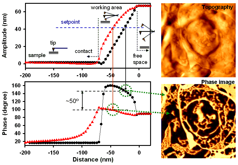
Our research utilizes phase‑shift imaging to visualize biological structures in unfixed rat brain sections as well as additives in polymer composites. Shown above are representative topographic and phase images (5 µm × 5 µm scan area) obtained from an unfixed rat brain section, along with corresponding amplitude- and phase-distance curves. The contrast observed in the phase images reflects differences in energy dissipation of the vibrating cantilever–tip system, which depend on the local mechanical properties of the probed regions.
Tip–sample interactions inherently encode information related to viscoelasticity, surface chemistry, and other interfacial properties. Because AFM measurements involve a two‑body interaction, both the sample and the probe influence the measured response. A key aspect of our work is the control of AFM tip surface chemistry. Silicon probes are intrinsically hydrophilic and therefore susceptible to contamination by “sticky” species such as organic residues and inorganic oxides. Modifying tip surfaces with hydrophobic coatings, including self‑assembled monolayers (SAMs), offers a promising strategy to mitigate these effects and improve measurement reliability.
SPM routinely resolves nanometer‑scale surface features owing to the sharp apex of silicon probes (typical radius ~10 nm). However, when surface features approach the size of the tip apex, geometric convolution occurs and image fidelity is compromised. In cases where the tip apex is larger than the surface features, the resulting image is dominated by the probe geometry rather than the true sample morphology. Recognizing and accounting for this effect is essential for the correct interpretation of AFM images, particularly at the nanometer scale.
Time-of-flight secondary ion mass spectrometry
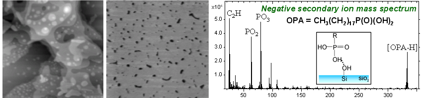
Time‑of‑flight secondary ion mass spectrometry (ToF‑SIMS) is a powerful surface‑analysis technique that identifies molecular species by measuring the mass‑to‑charge ratios (m/z) of secondary ions generated by bombardment of a surface with a focused primary ion beam (e.g., Bi3+). By detecting molecular ions and characteristic fragment ions, ToF‑SIMS is widely used for verification and identification of surface contaminants.
A common example is silicone oil (polydimethylsiloxane), which produces a characteristic set of secondary ion fragments that serve as diagnostic fingerprints. In the positive ion mode, these include ions at m/z 28, 73, 147, 207, 221, and 281, corresponding to Si+, SiC3H9+, Si2C5H15O+, Si3C5H15O3+, Si3C7H21O2+, and Si4C7H21O4+, respectively).
By incorporating an additional sputter ion gun, ToF‑SIMS can perform depth profiling, enabling characterization of thin oxide layers on metals and layered structures in electronic and optical films. The technique also offers strong imaging capabilities: a full mass spectrum is acquired at each pixel within a rastered area, allowing ion‑specific images to be generated by plotting signal intensity as a function of position.
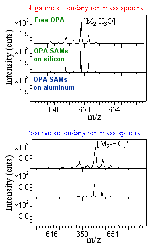
Beyond compositional analysis, ToF‑SIMS can be used to investigate how molecules attach to substrates by analyzing fragmentation pathways and molecule–substrate associations. For example, in studies of octadecylphosphonic acid (OPA, also known as ODPA) SAMs deposited on silicon and aluminum oxides, ToF‑SIMS reveals distinct ion fragmentation behaviors. On silicon oxide, condensed dimer species such as [M2-H2O]- and [M2-HO]+ (where M = C18H39PO3) are observerd, whereas these fragments are absent on aluminum oxide. OPA powders—representing free molecules bonded through hydrogen bonding between headgroups and van der Waals interactions among alkyl chains—exhibit fragmentation patterns similar to those of OPA SAMs on silicon oxide. This similarity suggests that OPA molecules form hydrogen‑bonded assemblies on silicon oxide surfaces. In contrast, the absence of condensed dimers and other fragmentation differences on aluminum oxide provide compelling evidence for covalent bonding of OPA SAMs to aluminum oxide substrates.
Self-assembled monolayers (SAMs)
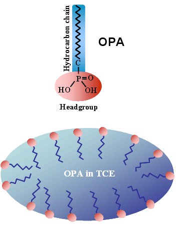
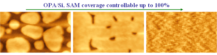
Using non‑polar solvents with dielectric constants of approximately 4, we have developed a novel method for delivering OPA SAMs onto hydrophilic surfaces. As illustrated in the schematic shown to the right, the solvent—trichloroethylene (TCE)—acts as an active medium that drives the concentration of molecular headgroups at the solvent interface. This mechanism promotes rapid SAM formation and enables the creation of monolayers that are either hydrogen‑bonded or covalently bonded to oxide surfaces, depending on the nature of the headgroup–substrate interaction. An example of achieving full‑coverage OPA SAMs on silicon oxide through solution addition during spin‑coating is shown below.
Because this solvent‑assisted approach requires only physical contact between the OPA‑loaded medium and a hydrophilic substrate, it enables exceptionally fast SAM growth and facilitates the spin‑coating of SAMs onto hydrophilic surfaces. The utility of this method has been demonstrated by other researchers, particularly in the modification of gate dielectric surfaces prior to deposition of active organic semiconductors in organic thin‑film transistors (OTFTs), resulting in improved device performance.
Our overarching objective in this research area is molecular‑level surface engineering using self‑assembled monolayers and the exploitation of such precisely controlled interfaces to create patterned surface chemistries. These engineered surfaces are then used to manipulate chemical and biological interactions in a controlled and reproducible manner.
Updated on March 29, 2026.